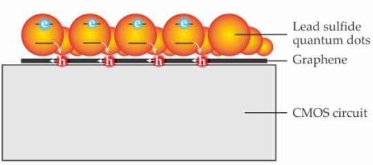
At the heart of a smartphone camera is CMOS circuitry that registers the electrons produced when visible light strikes a silicon wafer. Other semiconductors coupled to CMOS circuits could enable cameras to image in the UV, IR, and terahertz bands; such detectors could see applications for night vision, food inspection, environmental monitoring, and more. Now a research team led by Gerasimos Konstantatos and Frank Koppens of the Institute of Photonic Sciences (ICFO) in Barcelona, Spain, has taken the first steps toward that possible future: It has coupled a graphene–quantum dot photodetector to a CMOS circuit to create an imaging chip sensitive to wavelengths ranging from 300 nm to 1850 nm. (The group’s earlier related work was discussed in Physics Today, July 2012, page 15.)
![]()
© 2026 leventparali.com.tr
All Rights Reserved.
| Visitor Counter | ||||||
| » 1 Online | » 17 Today | » 67 Yesterday | » 17 Weekly | » 2545 Monthly | » 16357 Yearly | |
| » Total Number Of Visitors 163590 | ||||||